
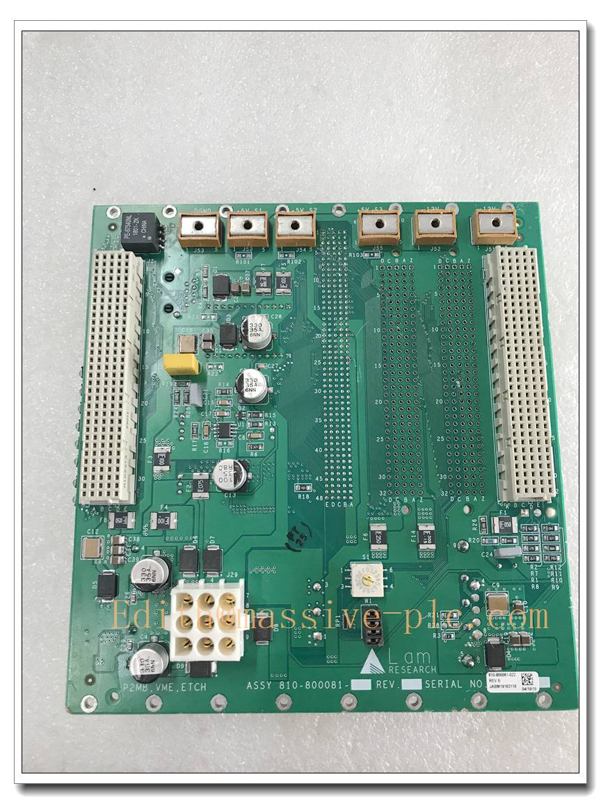
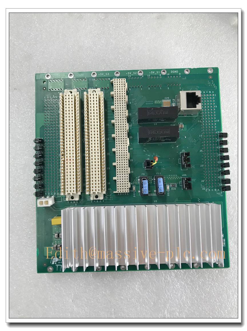
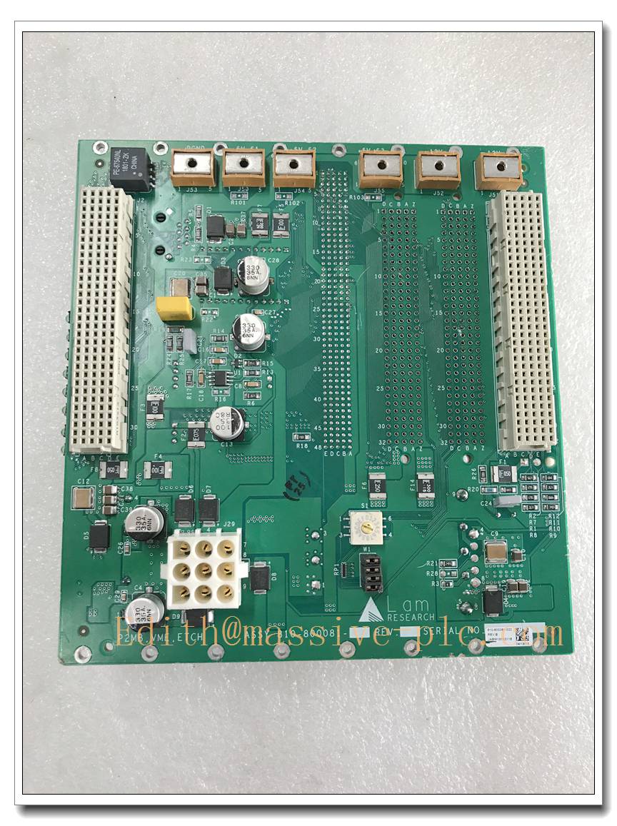
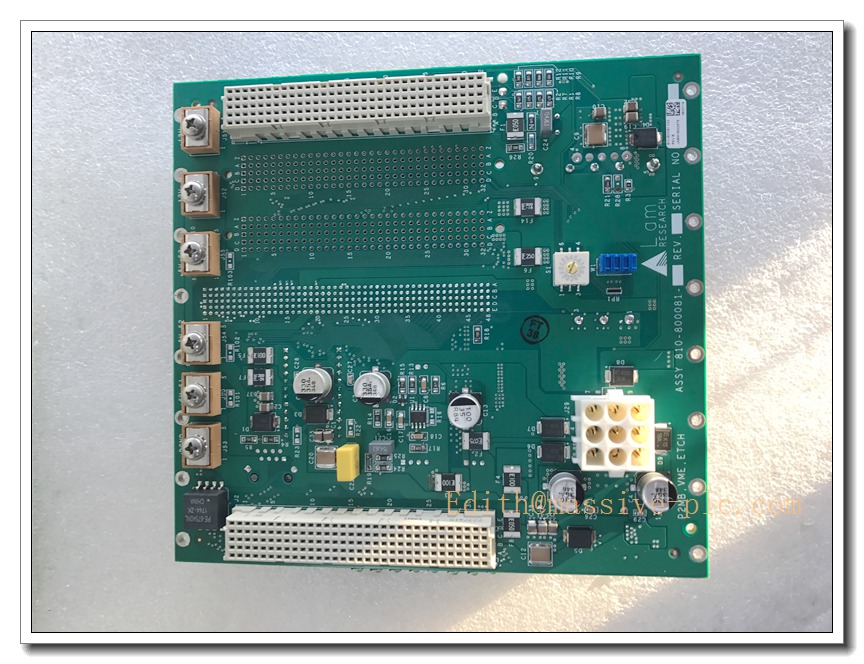
Description
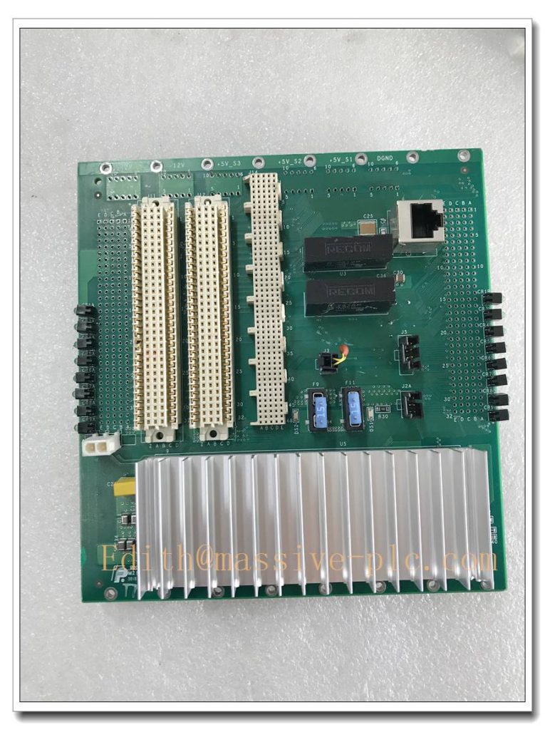
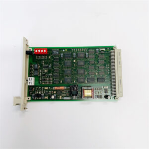
LAM 810-800081-022 Pulse Power Sample & Hold VME PCB, Plasma Pulsed RF Sampling Board for Semiconductor Etch Chamber
Product Description
The 810-800081-022 is a VME-formatted pulse power sample and hold PCB engineered by Lam Research for pulsed RF plasma etch platforms. It captures, locks and samples transient high-speed voltage/current waveforms from pulsed RF power delivery subsystems during plasma cycling. The board holds instantaneous pulse power readings for digitization by the chamber controller, enabling closed-loop tuning of RF pulse timing, duty cycle, peak power and plasma impedance. Circuitry is conformal-coated to resist cleanroom humidity, fluorine-based plasma byproducts and cabinet vibration. It is a mission-critical spare for diagnosing pulsed RF instability, waveform distortion and power regulation faults on compatible Lam etch systems.
Technical Parameters
| Item | Specification |
|---|---|
| Manufacturer | Lam Research |
| Model | 810-800081-022, Pulse Power Sample & Hold VME PCB |
| Function | Pulsed RF Waveform Capture, Sample & Hold, Transient Power Sampling |
| Form Factor | VME bus card |
| Power Supply | 24 VDC auxiliary cleanroom supply; isolated analog reference rails |
| Signal Interface | High-speed differential RF sense inputs; VME host backplane communication |
| Diagnostics | Signal saturation detection, reference offset drift, VME bus timeout, over-range pulse detection |
| PCB Protection | Conformal coating for corrosive process byproduct resistance |
| Mounting | VME chassis slot in RF cabinet |
| Operating Temperature | 15 ℃ ~ 60 ℃ |
| Humidity | 10–85% RH, non-condensing |
| Compliance | SEMI S2 semiconductor equipment safety standard |
| Weight | Approx. 0.34 kg |
| Status Indicator | LEDs for power, VME bus activity, sample trigger and signal saturation fault |
Recommended Related Models (8 units)
- 810-800081-012: Earlier revision of pulse power sample & hold VME PCB
- 810-800082-310: Alternate channel pulse power sample and hold board
- 810-114278-001: RF Match Control Board for ICP plasma source
- 810-066590-004: Chamber Analog Interface PCB for process sensor conditioning
- 810-046015-010: Gas Box MFC Interface PCB for process gas control
- 853-049542-173: 24-channel temperature control node PCB
- 61-428059-00: VECTOR EXTREME EIOC 1 Chamber I/O & Motion Controller
- Pulsed RF Generator Assembly: RF power source paired with this sampling board
810-800081-022
Compatibility & Installation Traps
Compatibility
- Primary host platforms: Lam Research VECTOR EXTREME, Kiyo pulsed plasma etch systems
- Control software: Lam fab host pulsed RF recipe editor and power fault monitoring framework
- Field devices: Pulsed RF generator, directional couplers, high-speed voltage/current sense probes
- Note: Implements Lam proprietary VME bus protocol; it cannot be substituted with generic VME data acquisition cards.
Critical Installation Traps
- Revision & Firmware Matching: Board revision and FPGA firmware must match tool software. Mismatch results in corrupted pulse waveforms, incorrect power calculation or RF recipe abort.
- High-Speed Sense Polarity: Reversed differential RF sense lines invert captured waveforms and produce false impedance and peak power readings, destabilizing plasma.
- Conformal Coating Integrity: Avoid scratching conformal coating during ESD handling. Damaged coating exposes high-speed analog traces to corrosive fluorine byproducts and causes intermittent waveform drift.
- Extreme ESD Sensitivity: High-speed sample/hold capacitors and front-end amplifiers are highly ESD-sensitive. All service must be performed in an ESD-controlled cleanroom workstation.
- Isolate RF Sense Lines Before Power-Up: A shorted RF coupler or sense harness can destroy the board’s delicate analog front-end. Disconnect field sense cables before energizing the replacement PCB.
- VME Connector Pin Integrity: Bent VME edge connector pins trigger intermittent bus or sampling faults that are difficult to replicate on bench static testing.
- Cleanroom Handling Rules: Never touch PCB traces or connector pins with bare hands. Skin oils degrade high-frequency signal integrity under thermal cycling.
- Post-Replacement Waveform Calibration Mandate: After swap, perform offset calibration, gain calibration and pulse trigger alignment. Skipping calibration leads to inaccurate RF power control and poor etch uniformity.
Standard Operating Procedure (SOP)
- Pre-installation inspection: Inspect PCB, VME edge connector and conformal coating for scratches or corrosion. Confirm part number and revision against chamber BOM.
- Lockout and energy isolation: Place tool in safe state, purge chamber gases, de-energize RF generator and VME chassis 24VDC auxiliary power, apply lockout/tagout.
- Mechanical removal: Remove VME cabinet panels, disconnect high-speed RF sense harness and VME backplane. Extract old sample & hold PCB from its assigned slot.
- Reassembly and cabling: Insert replacement PCB into VME slot and secure fasteners. Reconnect RF differential sense cables, verify pin assignment and fully latch connectors.
- Power-up and self-test: Restore 24VDC auxiliary power. Verify power and VME bus LEDs. Run built-in channel offset and trigger diagnostic tests.
- RF waveform calibration: Complete gain, offset and trigger timing calibration. Confirm captured pulse waveforms match golden reference traces within tolerance.
- Process qualification: Execute dry plasma pulsed RF recipes, monitor peak power, impedance and pulse stability. Release to production only after passing RF process qualification.
- Decommissioning: Isolate power before removal. Cap high-speed signal connectors and pack defective PCB in ESD shielding bags for failure analysis or controlled disposal.
Application Scenarios
- High-speed transient waveform sampling for Lam pulsed RF plasma etch subsystems
- Sample & hold capture of RF voltage, current and impedance during pulsed plasma cycles
- Closed-loop pulsed RF power, duty cycle and plasma impedance tuning
- Cleanroom semiconductor wafer pulsed plasma etch high-volume production
- Preventive maintenance replacement of aging pulse power sampling PCBs
- Troubleshooting intermittent RF waveform distortion, power drift and pulse trigger faults
- RF power metrology subsystem spare stocking and chamber retrofit
- Advanced pulsed recipe optimization for high aspect ratio etch processes
Supporting Components
- ESD wrist strap, ESD mat and anti-static shielding bags for cleanroom service
- Torque screwdriver set for VME card mounting fasteners
- Replacement VME edge connector contacts and RF differential sense harness
- Lam tool service software and service login credentials
- Conformal coating touch-up repair kit
- RF waveform reference calibrator and high-speed oscilloscope verification fixture
- Filtered 24VDC cleanroom power supply with surge protection
- Pulsed RF directional coupler and voltage/current sense probe assemblies

 Start Chat