
Description
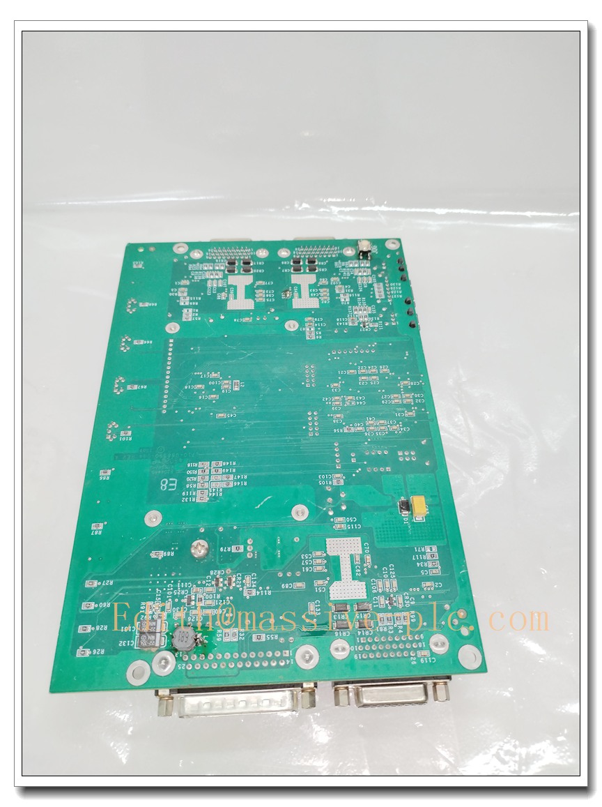
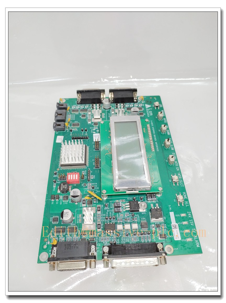
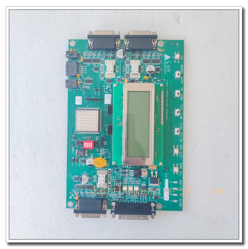
LAM 810-066590-004 Chamber Analog Interface PCB, Semiconductor Etch Analog Signal Conditioning Board
Product Description
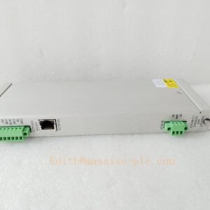
The 810-066590-004 is a precision analog interface printed circuit board designed for Lam Research plasma etch chamber subsystems. It conditions low-level analog signals from multiple process sensors, isolates noise from high-power plasma and RF circuits, and transfers scaled readings to the chamber main controller. The board also receives analog setpoint commands from the host and drives auxiliary process control components. All circuitry is protected by conformal coating to withstand cleanroom conditions including fluorine-based plasma byproducts, moisture and mechanical vibration. It is responsible for pressure transducer signal acquisition, analog reference generation and noise filtering, serving as a critical spare for resolving analog signal instability and sensor communication faults on compatible Lam etch platforms.
Technical Parameters
| Item | Specification |
|---|---|
| Manufacturer | Lam Research |
| Model | 810-066590-004 |
| Function | Chamber Analog Signal Conditioning & Interface PCB |
| Power Supply | 24 VDC cleanroom auxiliary supply; isolated precision 5 V analog reference rail |
| Signal Type | 4–20mA / 0–5V analog input for pressure and process sensors; analog output for auxiliary setpoint control |
| Host Interface | Lam proprietary internal cabinet backplane bus |
| Diagnostics | Signal out-of-range detection, sensor open/short circuit, reference rail fault, noise anomaly logging |
| PCB Protection | Conformal coating for resistance to corrosive process byproducts |
| Mounting | Plug-in slot inside chamber control cabinet |
| Operating Temperature | 15 ℃ ~ 60 ℃ |
| Humidity | 10–85% RH, non-condensing |
| Compliance | SEMI S2 semiconductor equipment safety standard |
| Weight | Approx. 0.22 kg |
| Status Indicator | LED indicators for power, bus communication and analog channel fault status |
Recommended Related Models (8 units)
- 810-066590-001: Earlier base revision of this analog interface PCB
- 810-046015-010: Gas Box MFC Interface PCB for gas flow control
- 853-049542-173: 24-channel temperature control node board
- 810-102361-222: Rocker Valve Interface PCB for vacuum sequencing
- 853-150806-001: OES Optical Emission Spectrometer for plasma endpoint detection
- 810-114278-001: RF Match Control Board for ICP plasma source
- 61-428059-00: VECTOR EXTREME EIOC 1 Chamber I/O & Motion Controller
- Capacitance Manometer Pressure Gauge: Process pressure sensor paired with this analog board
Compatibility & Installation Traps
Compatibility
- Primary host platforms: Lam Research VECTOR EXTREME, Kiyo and 2300 Flex plasma etch systems
- Control software: Lam fab host process monitoring and recipe execution framework
- Field devices: Capacitance manometers, chamber pressure transducers and other analog process sensors
- Note: Uses Lam proprietary backplane bus; not compatible with standard off-the-shelf analog PLC modules.
Critical Installation Traps
- Revision and Firmware Matching: Hardware revision and onboard firmware must match the tool software configuration. Mismatch can cause offset errors, unreadable sensor signals or recipe holds.
- Analog Wiring Polarity: Reversed sensor wiring will produce inverted readings and false pressure alarms, disrupting chamber pressure regulation during etch recipes.
- Conformal Coating Integrity: Avoid scratching conformal coating during ESD handling. Damaged coating exposes traces to corrosive fluorine byproducts and leads to intermittent signal drift.
- High ESD Sensitivity: Precision analog amplifiers and reference components are susceptible to electrostatic discharge. All handling must occur within an ESD-controlled cleanroom workstation.
- Field Sensor Isolation Before Power-Up: A shorted transducer cable can damage the board’s analog front-end. Disconnect field sensor harnesses before energizing the replacement PCB.
- Backplane Connector Pin Care: Bent edge connector pins create intermittent signal faults that are difficult to reproduce in static bench tests.
- Cleanroom Handling Rules: Never touch PCB traces or connector pins with bare hands. Skin oils degrade insulation and introduce measurement drift under thermal cycling.
- Post-Install Analog Calibration Required: After replacement, sensor zero and span calibration must be performed. Skipping calibration results in inaccurate chamber pressure readings and poor process performance.
Standard Operating Procedure (SOP)
- Pre-installation inspection: Examine PCB, edge connector and conformal coating for scratches or corrosion. Confirm part number and revision against the chamber BOM.
- Lockout and energy isolation: Set the tool to safe state, purge chamber process gases, de-energize chamber 24VDC auxiliary power and apply lockout/tagout.
- Mechanical removal: Remove cabinet access panels, disconnect backplane bus and analog sensor field harnesses. Extract the old analog interface PCB from its assigned slot.
- Reassembly and cabling: Insert the replacement PCB into the backplane slot and secure mounting fasteners. Reconnect all sensor cables, validate pinout and lock all connectors.
- Power-up and self-test: Restore 24VDC auxiliary power. Verify power and bus LEDs are active. Run the tool’s built-in analog channel continuity diagnostic.
- Analog loop calibration: Perform zero and span calibration for all connected pressure transducers. Confirm measured values match reference gauges within specified tolerance.
- Process qualification: Execute dry chamber cycles, monitor pressure stability and alarm behavior. Release to production only after passing pressure control qualification.
- Decommissioning: Isolate power before removal. Cap all connectors and pack the defective PCB inside an ESD shielding bag for failure analysis or controlled disposal.
Application Scenarios
- Chamber analog sensor signal conditioning for pressure transducers and capacitance manometers
- Noise isolation of low-level process measurements from high-power RF and plasma interference
- Analog reference generation and scaled signal transmission to the chamber main controller
- Cleanroom semiconductor wafer plasma etch production
- Preventive maintenance replacement of aging analog interface PCBs
- Troubleshooting of intermittent pressure drift, noisy sensor signals and out-of-range alarms
- Chamber analog measurement subsystem spare inventory and retrofit
- Recipe pressure profile tuning to stabilize plasma etch conditions
Supporting Components
- ESD wrist strap, ESD mat and anti-static shielding bags for cleanroom service
- Torque screwdriver set for PCB mounting fasteners
- Replacement edge connector contacts and chamber analog sensor wiring harness
- Lam tool service software and service login credentials
- Conformal coating touch-up repair kit
- Reference pressure calibration standard for transducer verification
- Filtered 24VDC cleanroom power supply with surge and short-circuit protection
- Spare capacitance manometer pressure transducer assemblies

 Start Chat